:quality(80)/p7i.vogel.de/wcms/53/fb/53fb719e1b7ca51e26a600beb4973caa/0117927695.jpeg "In extreme cases, the overheating of a power supply unit can lead to a fire, especially if other safety mechanisms such as overcurrent protection fail or are not present. It is therefore important to recognize overheating symptoms at an early stage and take appropriate countermeasures. (Source: DALL-E )")
:quality(80)/p7i.vogel.de/wcms/20/5f/205f55e131397019d7d0b4c93afd7692/0117866888.jpeg "Black light control of the ZEISS projection optics for the High-NA-EUV lithography. The heart of the lithography machine consists of more than 40,000 parts and weighs around twelve tons. (Source: Photo: Courtesy of ZEISS)")
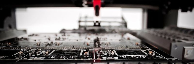
:quality(80)/p7i.vogel.de/wcms/8b/15/8b159540ecd785e6898feb8cbd658fe6/0117592369.jpeg "With advanced solid-state electronics inserted at the output stages for many radar RF chains, system engineers can set specifications to achieve improved range, resolution, and sensing capabilities. The article will discuss devices that minimize pulse droop to meet the demands of today’s high performance phased array radars. (Source: OpenAI's DALL·E)")
:quality(80)/p7i.vogel.de/wcms/b2/4f/b24f4455e347520465f1d2d37769666c/0117181551.jpeg "Both AC and DC describe types of current flow in a circuit. In direct current (DC), the electric charge (current) only flows in one direction. Electric charge in alternating current (AC), on the other hand, changes direction periodically. (Source: ATKWORK888 - stock.adobe.com)")
:quality(80)/p7i.vogel.de/wcms/9b/f4/9bf4c897c21cec0c927124f0b716f48d/0117966730.jpeg "From the 11 - 13 June 2024, the PCIM Europe will once again open its doors for numerous exhibitors and visitors. Read more about this years conference here. (Source: Mesago Messe Frankfurt GmbH/ Uwe Mühlhäußer)")
:quality(80)/p7i.vogel.de/wcms/da/ff/daff35bdf441484576a996352b0b8b5e/0117868043.jpeg "Left: Atsushi Osaki, Representative Director and President, SUBARU CORPORATION
Right: Mritaka Yoshida, Director and President, AISIN CORPORATION (Source: AISIN CORPORATION)")
:quality(80)/p7i.vogel.de/wcms/e8/9b/e89bb20d9e91ad553544c02de49bd4e6/0117906392.jpeg "Tektronix and recently acquired EA Elektro-Automatik now offer expanded power portfolio for engineers who are electrifying our world . (Source: Nuthawut - stock.adobe.com)")
:quality(80)/p7i.vogel.de/wcms/02/90/02904be1b73021c4ccea3df7623ed156/0117603663.jpeg "In this article you will find tips on how to save money in the production of printed circuit boards. (Source: Pitchayaarch - stock.adobe.com)")
:quality(80)/p7i.vogel.de/wcms/df/6d/df6d4da46e35064efa91d9b8658131a0/0118004183.jpeg "RAAAM has developed the most cost-effective on-chip memory technology in the semiconductor industry, providing 50% area reduction over high-density SRAM and reduced power consumption by a factor of five. (Source: Johannes - stock.adobe.com)")
:quality(80)/p7i.vogel.de/wcms/3e/9e/3e9ed788776623d655ec51f92e151ef4/0117774205.jpeg "A masterpiece of modern semiconductor technology: The blue LED symbolizes the triumph over complex material and manufacturing challenges that have long made the development of efficient blue light-emitting diodes a challenging goal in electronics. (Source: Guy Pracros - stock.adobe.com)")
:quality(80)/p7i.vogel.de/wcms/35/f2/35f243dd4bd4d57587bd7e4f7a85d6fa/0117752002.jpeg "This article covers the basics of the photodiode. (Source: mat - stock.adobe.com)")
:quality(80)/p7i.vogel.de/wcms/af/5b/af5bedf666c192a3698fce3cf3f63211/0117691222.jpeg "The 17-step inverter simplifies the structure without compromising performance compared to traditional inverters. Learn more about it in this article. (Source: OpenAI's DALL·E)")
:quality(80)/p7i.vogel.de/wcms/a0/22/a0220573ab4987d56f248dd3d9712760/0117238956.jpeg "Technology Computer-Aided Design “TCAD'' is used to optimize the manufacturing process of semiconductors. (Source: Gorodenkoff - stock.adobe.com)")
:quality(80)/p7i.vogel.de/wcms/4e/13/4e1363ce48fc85e61d98a235969d4638/0116922802.jpeg "(Source: Hseyin - stock.adobe.com)")
:quality(80)/p7i.vogel.de/wcms/70/14/7014ecedef4954eb2b455e5a522804b7/0102877609.jpeg "dSPACE provides comprehensive end-to-end solutions for developing and testing e-mobility and e-drive applications – to shape and master the rapid transition to electromobility together with their customers. (Source: © dSPACE GmbH)")
:quality(80)/p7i.vogel.de/wcms/8d/a5/8da5b7876ca5418c7a6666a4b6fe01ed/0116529715.jpeg "For the first time, high-fidelity thermal simulation data can be shared in the electronic supply chain while protecting semiconductor OEM’s intellectual property. (Source: Noah - stock.adobe.com)")
Research & Development Is gallium nitride (GaN) the silicon of the future?
A power struggle is underway in the world of electronics. Faster, more efficient gallium nitride semiconductors have already usurped traditional silicon MOSFETs in a variety of applications. But is GaN really ready to take the throne?
Related Vendors
:fill(fff,0)/p7i.vogel.de/companies/62/95/6295c25c8dc1a/schunk-sonosystems-300dpi.png "schunk-sonosystems-300dpi (Schunk)")
:fill(fff,0)/p7i.vogel.de/companies/60/21/60214fbbcc5e0/index.png "index.png (Kundenwebsite)")
What’s gallium nitride (GaN)?
Gallium nitride is a direct bandgap semiconductor material used to manufacture semiconductor devices such as transistors and diodes. This high-performance compound first hit the power electronics market in the 1990s as a vital component in light emitting diodes (LEDs). GaN has a particularly wide bandgap of 3.2 eV, making it capable of handling very high voltages and operating at high temperatures.
It can be used for a wide range of applications—from optoelectronic devices to high-frequency radio communications—and new uses are constantly being found for this efficient, highly powerful semiconductor material.
Current GaN applications include:
- Lasers and photonics applications such as light-emitting diodes (LEDs)
- Solar cells for photovoltaic systems
- Radiation-hardened transistors for satellites
- Radio frequency components such as RF power amplifiers
- Wireless power transmission, e.g. wireless chargers for phones, laptops, game console controllers, heart pumps and other medical applications
- DC-DC converters for datacom applications, e.g. server farms and centralized telecommunications centers
- LiDar (light detection and ranging), e.g. devices in autonomous cars that meas-ure distances using lasers
- Imaging and sensing, e.g. power amplifiers for microwave and terahertz (ThZ) devices
GaN vs. silicon
Before GaN took off, silicon had long been the most widely used material for manufacturing semiconductors. The invention of the silicon MOSFET (metal-oxide-silicon fieldeffect transistor) revolutionized computing and paved the way for the digital age. Now, after decades of dominance, it appears that silicon may have peaked. According to gallium nitride experts GaN Systems, “we are reaching the theoretical limit on how much silicon MOSFETs can be improved, how power-efficient they can be”.
A look at the properties and capabilities of the two semiconductors does suggest that the high-performance newcomer will eventually supersede silicon. When comparing GaN and silicon, the bandgap is a good place to start. GaN’s bandgap is 3.4 eV, whereas silicon has a value of just 1.12 eV. This means GaN semiconductors can sustain higher voltages and survive higher temperatures than silicon MOSFETs. The current can travel faster through GaN semiconductors, ensuring greater efficiency and fewer switching losses when they are used in hardswitching applications. They have less capacitance than silicon MOSFETs, which means that less power is lost when devices are charged and discharged. GaN semiconductors also take up less space on circuit boards, making it possible to manufacture ever-smaller electronic appliances.
:quality(80):fill(efefef,0)/p7i.vogel.de/wcms/5f/fe/5ffed0cad9749/2.jpg "2.Winner_PCIM 2020")
Cost is another key factor. It is possible to grow gallium nitride crystals on top of silicon, so they can be produced in existing silicon manufacturing facilities and do not require costly specialized production sites. Although gallium nitride crystals are currently still more expensive to produce than silicon, GaN semiconductors lower a system’s overall production costs by reducing the size and cost of other components.
GaN semiconductors’ superior speed and efficiency also make them better suited to meeting the environmental pollution regulations that are required to mitigate climate change.
Is there anything GaN can’t do?
As far as semiconductor devices go, GaN appears to tick all the boxes. Yet despite its widespread use in a variety of industries, there are still several applications that it has yet to master.
While GaN semiconductor devices have become indispensable for optoelectronic and high-frequency applications, for example, GaN transistors are not yet as versatile as silicon MOSFETs. The problem lies in the fact that most GaN transistors are depletion-mode or “normally-on” transistors. According to Power Electronics magazine, “deple-tion-mode transistors are inconvenient because at start-up of a power converter, a negative bias must first be applied to the power devices or a short circuit will result”. There is also the fact that electronic circuitry typically requires both depletion-mode and enhancement-mode transistors. However, workarounds for this issue have already been developed and it is surely only a matter of time before GaN semiconductors will appear in even more products and industries.
(ID:46300273)
:quality(80)/p7i.vogel.de/wcms/3d/44/3d444b76b18adb027cfd56e88d96c689/0117052006.jpeg "Known as vertical GaN membrane transistors, these power devices will combine the efficiency of wide-bandgap semiconductors with the lower cost of already established silicon semiconductor technology. (Source: Sashkin - stock.adobe.com)")
:quality(80)/p7i.vogel.de/wcms/67/a9/67a9bfa6e215f2657331765672a43be5/86165585.jpeg "Semiconductors are essential for power electronics. (Source:Public Domain)")